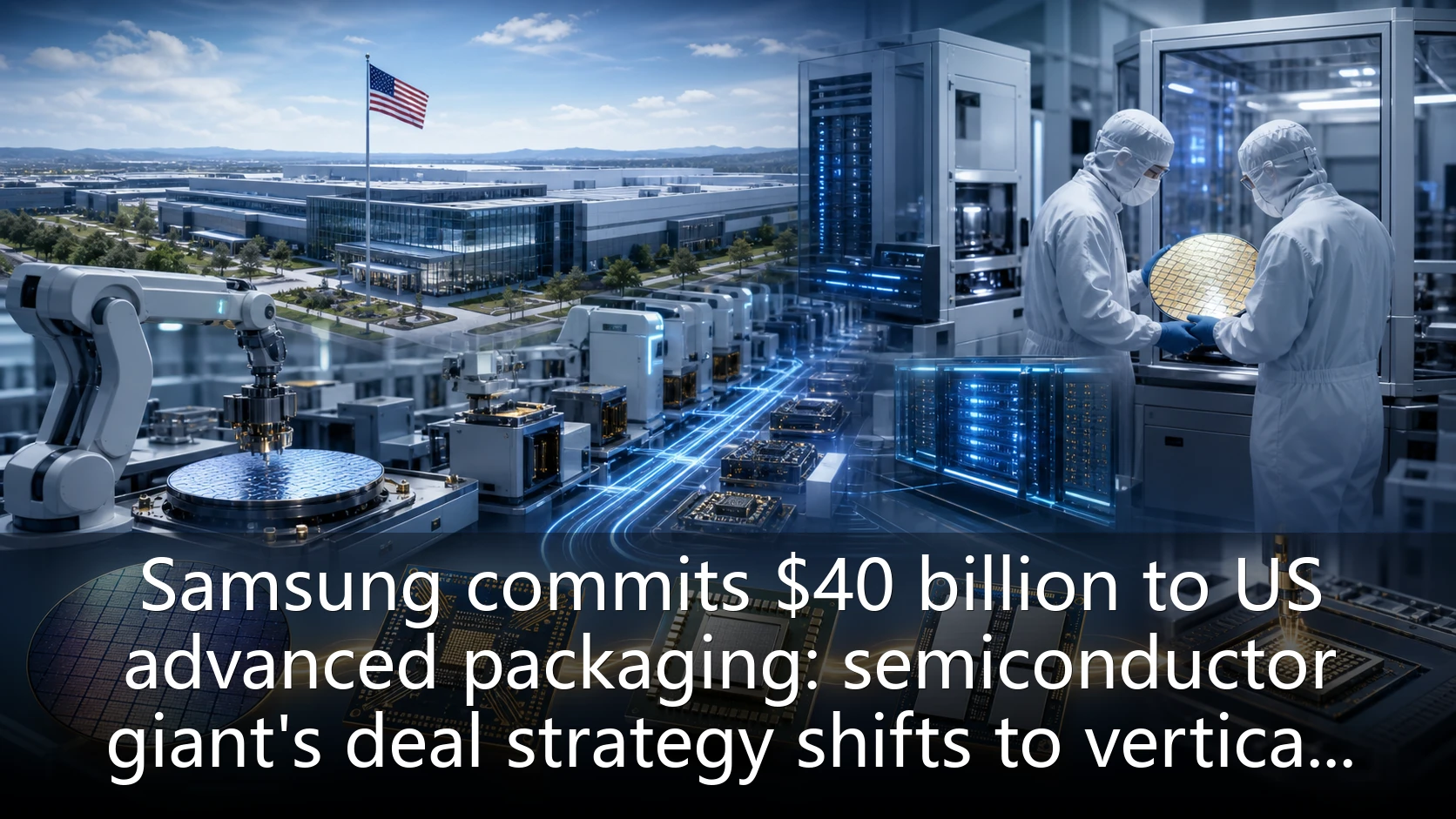
July 28, 2026, Seoul – Samsung Electronics today announced a major investment plan that shocked the global semiconductor industry: it will invest $40 billion to build a new advanced packaging factory in Taylor, Texas, and simultaneously reach a strategic cooperation with Google to jointly develop next-generation custom AI chips. This move marks Samsung's radical shift from pure manufacturing to vertical integration in its semiconductor transaction strategy, directly challenging the monopoly of TSMC and Intel in the advanced packaging field.
Investment Details and Strategic Intent
According to Samsung's statement, the new factory will focus on 2.5D and 3D advanced packaging technologies, expected to start production in 2028 with an annual capacity meeting 10% of global advanced packaging demand. Kyung Kye-hyun, head of Samsung Electronics' Device Solutions Division, said in a press conference: "This investment is not only an expansion of capacity, but also Samsung's fulfillment of its commitment to 'end-to-end' chip solutions. We will provide customers with one-stop services from design, manufacturing to packaging and testing."
Notably, Samsung also announced a deep partnership with Google to customize AI accelerator chips based on Samsung's 3nm GAA process. Google will station a design team at the new factory to ensure synergistic optimization of chip and packaging processes. Analysts believe this move aims to lock in tech giants with long-term orders, avoiding a repeat of its previous over-reliance on a single large customer in the mobile SoC market.
Vertical Integration: New Deal Strategy of Semiconductor Giants
For a long time, the semiconductor industry followed a vertical division model of "design and manufacturing separation." However, in recent years, as Moore's Law has slowed and advanced packaging has become key to sustaining performance improvements, the vertical integration strategy has reemerged. Samsung's logic behind this investment is clear: controlling the advanced packaging segment will allow it to dominate key markets such as HBM (High Bandwidth Memory) and Chiplet. In fact, Samsung is already the world's second-largest semiconductor company, but its market share in advanced packaging is only about 15%, far behind TSMC's 65% and Intel's 10%.
"Samsung's $40 billion investment is a precise bet on the competitive landscape of the 'post-Moore era,'" commented Mark Li, chief analyst at industry research firm IC Insights. "It directly targets TSMC's CoWoS and Intel's Foveros technologies. If Samsung succeeds, it will change the power structure of the entire chip supply chain."
At the same time, this strategy is closely tied to Samsung's recent executive changes. In early 2026, Samsung Electronics appointed a former Intel executive as president of its advanced packaging business. The "integration route" led by this executive has already received preliminary cooperation intentions from multiple clients including Google and NVIDIA.
Deep Significance of Cooperation with Google
As one of the world's top three cloud computing providers, Google's demand for AI chips has exploded. Previously, Google's self-developed TPUs mainly relied on TSMC for foundry, but this shift to Samsung reflects the trend of tech giants diversifying supply chain risks and seeking customized services. According to the agreement, Samsung will provide Google with full-chain support from design optimization to packaging and testing, and promises to deliver the first custom AI chip based on 3nm GAA in 2027.
"Google needs to be more closely tied to the manufacturing process to ensure the unique competitiveness of its chips," said Rick Osterloh, Google's hardware chief, in a statement. "Samsung's vertical integration capabilities give us great confidence in future cooperation." This deal is expected to bring Samsung orders of over $5 billion annually, while strengthening its influence in the AI computing market.
Industry Competition Landscape Rewritten
Samsung's aggressive strategy immediately triggered a chain reaction in the industry. TSMC's stock price fell 4.3% after the announcement, and it urgently announced it would accelerate its 3nm factory expansion plan in Arizona, USA. Intel announced it would sign a five-year advanced packaging service contract with Amazon AWS, attempting to consolidate its "system-level foundry" positioning.
Notably, the US government welcomed this. The CHIPS Program Office of the US Department of Commerce issued a statement saying Samsung's investment "strengthens the resilience of the US domestic advanced chip supply chain" and is expected to receive up to $8 billion in federal subsidies. This also means that Samsung is leveraging geopolitical advantages to extend manufacturing capabilities to customers' doorsteps.
Future Outlook and Risks
Despite the attractive prospects, Samsung's deal strategy still faces multiple challenges: the huge $40 billion investment will take 5-7 years to break even, and advanced packaging technology iteration is extremely fast, with TSMC and Intel already accumulating a large number of patents in 3D stacking. In addition, increased reliance of major customers like Google on a single supplier may also raise antitrust concerns.
However, in the long run, the transaction strategies of semiconductor giants are shifting from "scale competition" to "ecosystem competition." By binding core customers through vertical integration while using US subsidies to reduce financial risk, Samsung's model may become a template for industry consolidation in the next decade.
As Kyung Kye-hyun said at the end of the press conference: "We are no longer just chip manufacturers, but the 'architects' of the digital revolution." Samsung's $40 billion bet is rewriting the rules of the global semiconductor industry.